

RESEARCH
OVERVIEW
Our research program covers a broad
variety of interdisciplinary topics under the overall
framework of Additive Manufacturing advanced through a
synergistic combination of computational design,
manufacturing and materials processing technologies, and
materials science. In all of our research endeavors and
collaborations, we strive to integrate these three key
elements together to achieve new fundamental scientific
insights, to produce groundbreaking high-impact results,
and to create innovative and disruptive Additive
Manufacturing technologies.
We synthesize diverse disciplines of science and
engineering to pursue our goals. They include the
following:
- Conception, design and implementation of leading edge, innovative and disruptive technologies for Additive Manufacturing.
- Design and construction of prototype and pre-commercial Additive Manufacturing machines and equipment.
- Selection, handling, processing, synthesis, preparation and characterization of feedstock materials for Additive Manufacturing.
- Multi-physics modeling, computational geometry, data structures and digital data processing algorithms for Additive Manufacturing.
- Energy delivery systems for Additive Manufacturing, including lasers, light sources, optics, and energy-material interactions.
- Feedback control systems for industrial production Additive Manufacturing.
- Qualification, Validation and Verification (QVV) procedures for industrial production Additive Manufacturing.
- Experimental materials characterization and theoretical property validation for Additive Manufacturing.
Overall, our research program is directed towards end-use applications in the Aerospace, Defense, Healthcare, Energy, and Nanotechnology sectors. Figure 1 below describes the defining research themes of my research group.
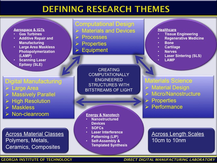
Fig. 1. Defining Research Themes in Georgia Tech's Direct Digital Manufacturing Laboratory
Some of the notable results achieved and future research plans in each of these areas are described below.
1. AEROSPACE & INDUSTRIAL GAS TURBINES
1.1 Additive Manufacturing of Ceramics for Direct Digital Investment Casting
Turbine airfoils with extremely complex internal cooling passages are produced through investment casting. The exterior airfoil shapes are defined by injection-molded wax patterns that are removed or “lost” after shelling. The internal cooling passages are defined by injection-molded ceramic cores that are removed or “lost” after casting. The core and wax molding operations require sophisticated tooling, leading to excessive initial and maintenance costs, very slow fabrication cycles, and low casting yields. Despite the maturity of current investment casting practices in the aerospace industry, a major challenge exists in the affordable, high-yield, production of cooled, single crystal nickel-superalloy airfoils for turbine engines. While many improvements in the performance of designs have been made, no significant improvements have been made to lower the cost of manufacturing turbine airfoils.
Large Area Maskless Photopolymerization (LAMP) is an additive manufacturing technology that was invented and developed at Georgia Tech with support from DARPA’s Disruptive Manufacturing Technologies program in a project titled “Direct Digital Manufacturing of Airfoils”. LAMP technology directly produces complex ceramic cores and integral-cored shell molds for airfoil investment casting from CAD files by selectively curing ceramic-loaded photocurable resins layer-by-layer. Layers are cured through the continuous projection of high-resolution bitmaps of UV light onto the resin in a scrolling and seamless manner, allowing for mass production. The molds are then thermally post-processed to a foundry-ready state for casting. Figure 2 shows the overall technical approach. LAMP eliminates nearly all the tooling, handling, and associated causes for scrap in the investment casting process, leading to dramatic reductions in lead-time, scrap rate, and ultimately cost. LAMP eliminates 3 major process steps in the conventional investment casting process chain through the direct digital manufacture of just cores, i.e. core injection molding tooling design, manufacture of core injection molding tooling, and injection molding of cores. However, in the direct digital manufacture of integral-cored shell molds, LAMP eliminates 7 major process steps through the elimination of all core injection and wax injection molding tooling, as well as core injection, wax injection, wax dipping, stucco coating, and wax meltout. Through a two-step binder burnout and firing process, LAMP-manufactured ceramic cores and integral-cored shell ceramic molds are plug-compatible with investment casting foundry practices. LAMP thus disrupts the current state-of-the-art investment casting process by disrupting not only the cost structure of conventional investment castings, but also the speed with which components can be fabricated.
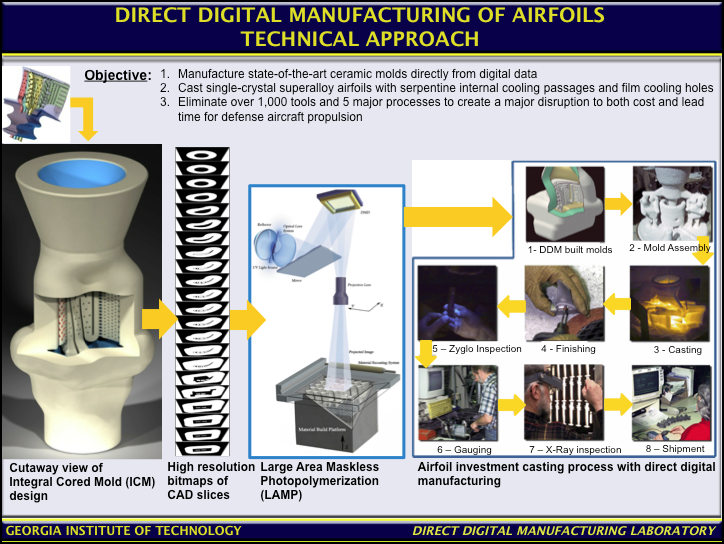
Fig. 2. Technical Approach to Direct Digital Manufacturing of Airfoils through LAMP technology.
My group at Georgia Tech has designed and built a laboratory scale LAMP Alpha machine with a build volume of 4" (X) x 4" (Y) x 6" (Z) and two production scale LAMP Beta machines with build volumes of 22" (X) x 22" (Y) x 12" (Z). My group has also worked closely with the group of Prof. John Halloran at the University of Michigan to develop both the materials and the process technology. To date, both uncored and integral-cored ceramic molds have been built. Equiaxed and single-crystal airfoil castings in the superalloys Inconel 718 and SC180 have been cast using these molds. Figure 3 shows integral-cored shell molds built in cutaway section, uncored molds, and uncored airfoil castings produced using these molds. These results illustrate the pathway that LAMP technology development is taking towards a disruptive manufacturing technology for producing cored single-crystal airfoils in a fraction of the time and at a significantly reduced cost when compared to the conventional investment casting process. LAMP technology is now being commercialized by DDM Systems, an Atlanta-based startup company that has an exclusive licensing agreement with Georgia Tech.
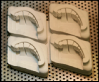
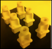
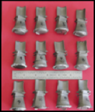
Fig. 3. Cut-away section of cored airfoil molds (left), uncored airfoil molds (middle), and uncored airfoil castings in IN718 superalloy produced through LAMP.
1.2 Future Research: Cyber-Enabled Manufacturing of Advanced Castings (CyMAC)
The next step in the evolution of the direct digital manufacturing of investment castings is the cyber-enabled manufacturing of advanced castings (CyMAC). Through CyMAC, my vision is to revolutionize the design, prototyping, rapid manufacturing, and rapid qualification of all investment castings made in the United States. LAMP technology has already demonstrated the potential to disrupt the state-of-the-art of investment casting through dramatic increases in the speed of ceramic mold manufacturing and will serve as the key enabler of this next revolution. I aim to accelerate the creation of a new and sustainable digital manufacturing paradigm that will pervasively reduce costs and lead times associated with all legacy and new investment castings. While continuing the research on next-generation LAMP technologies that promise further increases in build speed by up to 50X and revolutionary new capability to produce components with advanced designs considered conventionally non-manufacturable, I will pursue an integrated and synergistic technical approach that will combine the following four elements: Design, Manufacturing and Analysis Software Tools (CAx), Rapid Manufacturing Technologies, Rapid Qualification, and a Manufacturing Demonstration Facility for CyMAC. CyMAC will open up the design space and will enable the rapid manufacturing of advanced designs with complex geometries previously considered non-manufacturable. Figure 4 shows a schematic of CyMAC’s technical approach.
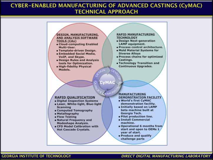
Fig. 4. Technical Approach to Cyber-Enabled Manufacturing of Advanced Castings (CyMAC).
1.3 Additive Manufacturing and Repair of High Value Metal Components via Scanning Laser Epitaxy
Fabrication techniques for making nickel-base superalloy components, particularly turbine blades, have evolved over the last half century from equiaxed casting to directionally solidified (DS) casting and more recently to single crystal (SX) casting with each improved technique resulting in higher operating temperatures. Both DS and SX casting are considered exotic techniques and have significant cost associated with hardware production. For example, SX turbine blades made using some of the most modern nickel-base superalloys such as CMSX-4 can cost several hundreds to thousands of dollars per piece involving several iterations of prototyping and tooling development that consume several months to years before final production. Due to the extreme conditions under which such engines operate, turbine components undergo loss of material due to oxidation and subsequent spallation.
Currently employed techniques to rebuild lost material have several drawbacks: (a) the build-up is often limited to a thin layer of polycrystalline material, therefore it does not preserve the directionally solidified (DS) or single-crystal (SX) microstructure of the base material that has been eroded away; (b) the material used for build-up is often of a different, lower performance alloy composition because the nickel-base superalloy comprising the hardware to be repaired is non-weldable or non-joinable; and (c) Lack of adequate thermal control leads of cracking and the formation of misoriented grains due to the fact that superalloys are susceptible to strain-age cracking and liquation cracking. Due to the high costs associated with making production quality hardware, turbine engine manufacturers are investigating ways to: (a) develop techniques to repair and restore damaged equiaxed, DS, and SX superalloy components to pristine condition, and (b) produce small lots of functional parts for prototyping and testing. Figure 5 below describes my group's technical approach combining physical modeling, experimentation, and characterization to achieve region-specific microstructure control in additively manufactured and repaired nickel-base superalloy components for turbine engines.
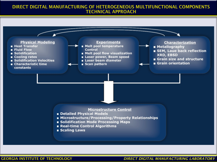
Fig. 5. Technical Approach to Direct Digital Manufacturing of Heterogeneous Multifunctional Components (HMCs) through Scanning Laser Epitaxy (SLE).
My group has designed, developed and implemented a workstation for conducting scanning laser epitaxy (SLE), a laser materials processing technique developed as part of ongoing research sponsored by the Office of Naval Research. This workstation is shown below in Figure 6. The workstation includes a continuous wave Nd:YAG laser, controlled atmosphere process chamber with substrate fixture and thermocouple array, galvanometer driven scanner and optics, and a process control cabinet. We have recently added a Ytterbium fiber laser to replace an older Nd:YAG laser, a high resolution thermal imaging camera, a video microscope for melt pool imaging. Work is ongoing to implement a real-time adaptive feedback control system for melt-pool temperature control.
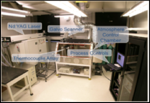
Fig. 6. Materials processing workstation for the SLE process developed with ONR support.
My group has demonstrated the ability to successfully produce fully dense, crack-free and defect-free monolithic deposits from nickel superalloy powders on substrates of the same composition in both polycrystalline MARM-247 and single-crystal CMSX-4 superalloys through SLE. A thorough investigation of SLE process parameters including laser power and scan speed has been conducted to determine their influence on the rebuilt microstructure and the degree of melt-back in the parent substrate. In the CMSX-4 single crystal deposits, the primary dendrite arm spacing is approximately 10-30 times finer than that of the parent substrate (shown in Figure 5). Particularly in the case of single-crystal components, such a fine microstructure is unattainable in components manufactured through traditional investment casting. The benefit of such a fine microstructure is that the overall component is generally more homogenous from the standpoint of the distribution of the alloying species and should thus result in superior performance and properties over that of the “as cast” component. Figures 7 and 8 below show representative specimens on MARM-247 and CMSX-4 deposited through SLE processing.
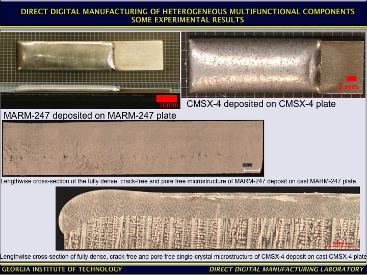
Fig. 7. Experimental Results on Scanning Laser Epitaxy of MARM-247 and CMSX-4.
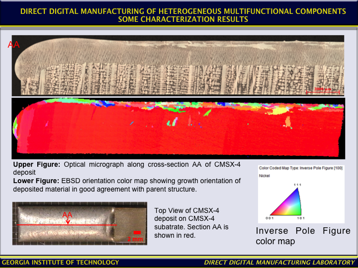
Fig. 8. Optical microscopy and electron-backscattered diffraction images of the longitudinal cross-section of a typical SLE-processed CMSX-4 sample. The coarser microstructure in the lower half is that of the investment-cast CMSX-4 plate substrate. The highly refined microstructure in the upper half is that of the laser-melted and resolidified CMSX-4 powder forming a fully dense deposit with a microstructure derived from epitaxial solidification. The majority of CMSX-4 deposited through SLE has [001] crystal orientation consistent with the investment-cast substrate. Some stray grains are present. The top of the deposit is encrusted with an equiaxed region due to high cooling rates and loss of thermal gradient.
Further investigations are ongoing to fully understand the origins of microstructure formation in SLE and its linkage to processing parameters. Further technological efforts are also ongoing in the areas of robust feedback control, SLE equipment design, and process automation to transition the SLE process to the DoD and its suppliers. The primary areas of investigation and development include: 1) Solidification modeling to obtain a deeper fundamental understanding of the mechanisms contributing to the microstructural transitions (e.g. columnar to equiaxed, oriented to misoriented). 2) Enhanced thermal control over the workpiece utilizing temperature distribution measurements from an infrared thermal imaging camera and an instrumented thermocouple array, coupled with knowledge of the mechanisms of microstructure formation, leading to better process control. 3) Utilization of electron microscopy tools (EBSD and TEM) to investigate grain orientation as a function of process parameters and the observation of gamma prime precipitates to further optimize the SLE process. 4) Development of mature SLE manufacturing process, equipment, and documentation for technology transition to DoD suppliers and repair facilities, with process knowledge tailored to the components and alloys of interest.
During my doctoral and post-doctoral work at UT, I designed and built two machines and was awarded two patents on direct laser fabrication techniques for making functional, fully dense components in high performance materials including nickel superalloys, titanium alloys, and superalloy cermets. Components produced on these machines were shown to exhibit equivalent or superior microstructures, chemistries, and mechanical properties in comparison to conventionally cast materials. Figure 9 shows examples of produced components: a titanium alloy (Ti-6Al-4V) guidance section housing for the Sidewinder missile and a MARM-247 superalloy-cermet abrasive turbine blade tip for a next generation fighter aircraft engine. Interestingly, the additive manufacturing of metal components through the layer-by-layer melting of metal powders using powerful scanning lasers has once again become an area of strong commercial interest, as all of the aerospace and industrial gas turbine companies strive to speed up the prototype, test and development cycle for new, higher efficiency engines. Thus, with funding from the Office of Naval Research, my group is initiating a research program to investigate the processing of nickel-base superalloys to produce functional fully dense components such as turbine airfoils through SLE conducted layer-by-layer.
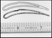
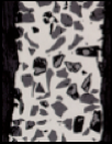
Fig. 9. (a) A titanium alloy Ti-6Al-4V guidance section housing for the AIM-9 Sidewinder missile, (b) Microstructure of fully dense Ti-6Al-4V, (c) MARM-247/CBN/Alumina superalloy cermet abrasive turbine blade tip, (d) Microstructure of fully dense cermet with uniform dispersion of CBN and Alumina particles in MARM-247 superalloy matrix.
1.4 Future Research: Cyber-Enabled Direct Digital Manufacturing of Heterogeneous Multifunctional Components (DDM of HMCs)
The next step in the evolution of SLE is the direct digital manufacturing of heterogeneous multifunctional components (HMCs) wherein material, microstructural, and property heterogeneity enables the performance of at least one function but more often multiple functions in addition to structural integrity. Multifunctional performance through heterogeneity can be imparted to a component through graded microstructure, graded composition, graded physical and chemical properties, or a combination of the above attributes. An example of a HMC is a jet engine turbine blade made of a nickel base superalloy with equiaxed, directionally solidified, or single-crystal microstructure having a ceramic thermal barrier coating (TBC) covering the airfoil surfaces and a ceramic-metal matrix composite material on the airfoil tip to serve as an abrasion resistant and oxidation resistant coating. A second example of a HMC is a turbine disk made of a monolithic superalloy composition with equiaxed microstructure but with radially graded grain sizes, with smaller grains at the hub enabling better tensile properties and larger grains towards the rim to enable superior creep strength and resistance to fatigue crack growth. A third example is a turbine disk made of two distinct superalloys and with a radial compositional gradient. A fourth example of a HMC is an integrally bladed rotor (IBR) with single crystal airfoils metallurgically bonded to a disc with equiaxed microstructure. A fifth and final example is a turbine blade with primarily single-crystal superalloy microstructure throughout the airfoil section but with a dual alloy attachment section, with a portion of the attachment section made of a polycrystalline superalloy to provide superior low cycle fatigue life at the attachment section. As indicated through the five examples cited above, transitions in microstructure, texture, composition, and properties in a HMC can be engineered over relatively small or large length scales compared to characteristic dimensions of the part, depending upon the functional gradient characteristics desired in a particular application. The direct digital printing of dry powders and well-dispersed nanomaterials to form smooth layers with spatially patterned heterogeneous materials followed by their consolidation through laser melting (DDM of HMCs) has the potential to create 3-D HMCs with entirely new functionality and characteristics that can meet or exceed the performance requirements being demanded of next-generation advanced high-performance materials. I plan to pursue research in the DDM of HMCs over the next several years.
2. HEALTHCARE
2.1 Additive Manufacturing for Tissue Engineering and Regenerative Medicine
Tissue engineering is an interdisciplinary field that combines engineering and the life sciences to develop techniques that enable the restoration, maintenance, or enhancement of living tissues and organs. A majority of these techniques utilize three-dimensional scaffold structures composed of natural or synthetic bioresorbable polymers. These scaffold structures are endowed with complex internal architecture, channels and porosity that provide sites for cell attachment and proliferation, as well as for conveying cells, growth factors and biomolecular signals to promote tissue regeneration at an implantation site. Tissue engineering has the potential to facilitate breakthrough therapies for repair of whole joints and organs. However, present fabrication methods have limited control over the geometry and porosity of scaffolds. In order to reconstruct complex joints such as the temporomandibular joint (TMJ), novel fabrication methods are needed to build complex, three-dimensional anatomically shaped scaffolds incorporating multiple biomaterials and porosity gradients that can enable the simultaneous growth and regeneration of multiple tissues (bone, ligament, cartilage or tendon), tissue interfaces and blood vessels.
My research in tissue engineering centers on devising novel additive manufacturing methods that can construct tissue engineering scaffolds with functionally tailored characteristics, notably geometry, material composition, and porosity. To date, we have investigated selective laser sintering to fabricate scaffolds in nylon-6, polycaprolactone (PCL), and polycaprolactone/hydroxyapatite composites. Figure 10 shows the technical approach to creating microarchitectured tissue engineering scaffolds using selective laser sintering of polymers and polymer-ceramic composites.
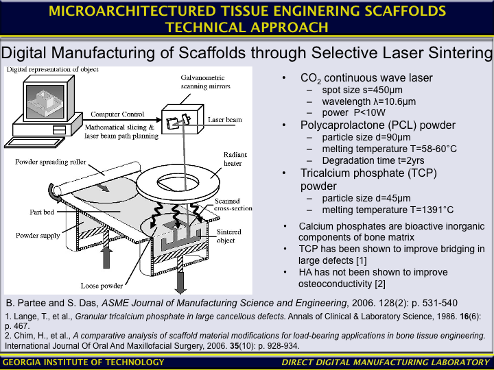
Fig. 10. Technical Approach to Digital Manufacturing of Tissue Engineering Scaffolds Through Selective Laser Sintering.
Figures 11-13 below illustrate some of the tissue engineering scaffolds that have been constructed and tested to date. Our investigations aim to design customized scaffolds by combining computational design techniques, patient specific computed tomography (CT) or magnetic resonance imaging (MRI) data and surgeon inputs, and then to fabricate the scaffolds using additive manufacturing techniques. We have successfully demonstrated in vivo bone regeneration on polycaprolactone scaffolds built by selective laser sintering combined with a gene therapy approach. Our future investigations aim to design, build and test multifunctional scaffolds for whole joints structures incorporating a bone scaffold, combined with a cartilage scaffold, and a ligament scaffold with different functional architectures and compositions, and seeded as needed with gradients of biofactors.
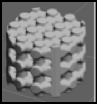
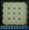
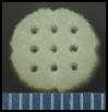
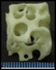
Fig. 11. (a) An 8mm cubic cellular scaffold design, (b) An 8mm diameter, 6mm high cylindrical cellular scaffold design (both with 800μm orthogonal channels and 1200μm pillars), (c) and (d) Nylon-6 scaffolds fabricated by SLS (scale in mm), (e) Biomimetic scaffold design derived from human proximal femur trabecular bone micro-CT data, and (f) Biomimetic scaffold fabricated in Nylon-6 by SLS.
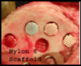


Fig. 12. (a) Implantation of cylindrical Nylon-6 scaffold into a Yucatan minipig mandible, (b) Volumetric rendering of scaffold micro-CT after 6 weeks showing bone ingrowth, (c) A cylindrical scaffold design with periodic interconnected porous architecture (12.5 mm diameter, 25.4 mm length, 2 mm pores) for mechanical tests, (d) Corresponding scaffold built in polycaprolactone by SLS (e) A scaffold design (5.0 mm diameter, 4.5 mm height, 1.5mm diameter pore) loaded with BMP-7 and implanted in immunocompromised mice to test bone regeneration, and (f) Micro-CT image of corresponding polycaprolactone scaffold removed after 4 weeks showing significant amounts of newly generated bone penetrating and encapsulating the scaffold.
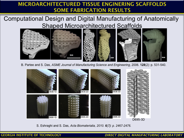
Fig. 13. 3D renditions and actual SLS processed PCL scaffolds. Top row: (a) a minipig mandibular condyle scaffold design, (b) & (c) two different human condyle scaffold designs incorporating 700 micron struts and 1.1-2mm pores. Bottom rows: Rectangular and cylindrical microarchitectured scaffolds for tensile and compressive mechanical property measurements as a function of scaffold pore architecture. Bottom far right: A micro-computed tomography reconstruction of a cylindrical scaffold for non-desctuctive visualization of interior architecture.
Figures 14 and 15 below illustrate some of our results on computational design and digital manufacturing of anatomically shaped microarchitectured scaffolds
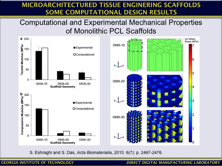
Fig. 14. Comparison between computationally predicted and experimentally measured mechanical properties of monolithic PCL scaffolds.
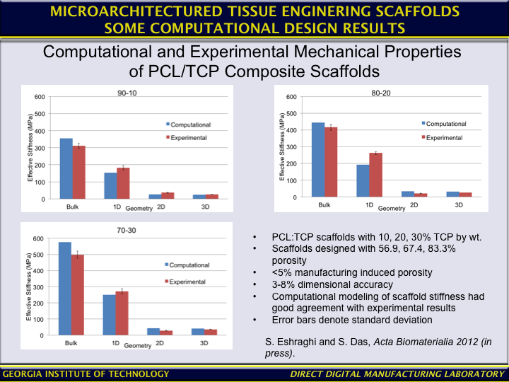
Fig. 15. Comparison between computationally predicted and experimentally measured mechanical properties of PCL/TCP scaffolds.
Figure 16 illustrates the applications and the impact of tissue engineering scaffolds with external anatomic shapes and internal microarchitecture with reference to specific example pertaining to repair and reconstruction of the temporo-mandibular joint.
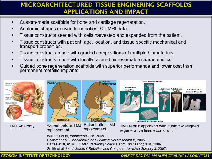
Fig. 16. Applications and impact of tissue engineering scaffolds with external anatomic shapes and internal micro architecture manufactured through selective laser sintering.
2.2 Future Research: Additive Manufacturing of Scaffolds with Encapsulated Cells for Cartilage Tissue Engineering
We aim to use LAMP technology to build hydrogel scaffolds with embedded microfluidic networks and encapsulated cells for cartilage tissue engineering. Previous attempts at the fabrication of large cartilage constructs have been plagued by poor nutrient transport to the interior of the tissue construct resulting in poor tissue growth and necrosis of the embedded cells. A microfluidic network embedded within the bulk of the construct may be able to meet the transport requirements of the interior cells but conventional manufacturing methods for scaffolds are—in most cases—limited to simple geometries and large feature sizes. LAMP is a cost-efficient, scalable technique for the fabrication of cartilage tissue scaffolds with a computationally designed microarchitecture. To fully realize its potential, the following research tasks will be pursued: 1) Systematic studies linking the hydrogel material composition and LAMP processing parameters to spatial resolution and material properties. 2) Development of computational design methods for cartilage tissue constructs taking into consideration mechanical and transport requirements. 3) Experimental characterization and validation of specimens made by computational design and digital manufacturing. 4) Implantation and testing of scaffolds in animal models.
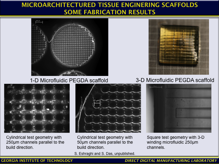
Fig. 17. Fabrication of PEG-DA hydrogel scaffolds for cartilage tissue engineering using LAMP technology.
3. ENERGY
3.1 Additive Manufacturing of Fuel Cells
Concern for energy conservation and for renewable energy sources has renewed interest in design and fabrication of fuel cells, micro-batteries, micro-combustors, micro-chemical reactors, , micro-channel based heat exchangers, solvent extractors, gas adsorption media, thermoelectric power devices, and catalytic structures. These devices have the potential for improved efficiency, energy density, compactness, portability and the integration of multiple functions. Each could portray significant commercial, military, societal and environmental value. With appropriate additive manufacturing methods, such devices could be fabricated with locally tailored material compositions optimized with respect to thermal, fluid, optical, chemical reaction or catalytic performance considerations.
My research in the area of fuel cells has focused on investigating novel methods for prototyping and manufacturing fuel cell components. In particular, my collaboration with Prof. Pravansu Mohanty (ME Department, UM-Dearborn) led to low cost rapid prototyping and rapid manufacturing techniques to make components for proton exchange membrane fuel cells (PEMFC). In a hybrid two-step process combining rapid prototyping and thermal spray deposition, first 3D printing and selective laser sintering techniques were used to produce low cost ceramic patterns with complex channel architectures. Second, thermal spray deposition techniques were used to deposit multiple materials layer-by-layer onto the sacrificial patterns for making functionally graded metallic bipolar plates for PEMFCs with improved corrosion resistance and electrical conductivity. Shown in figure 18(a) is the 3D CAD model of a pattern for a bipolar plate. Figure 18(b) is the actual pattern made in gypsum by 3D printing. Figure 10(c) shows the actual metallic bipolar plate with a Ni-Al to Molybdenum functional gradient, produced by thermal spray deposition onto the 3DP pattern.
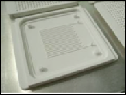
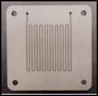
Fig. 18. (a) 3D CAD model of bipolar plate pattern, (b) Actual gypsum pattern made by 3D printing, and (c) Actual bipolar plate produced by thermal spray deposition of graded multilayers of fully dense Ni-Al and Molybdenum. The plate is 95mm square, with a 1mm square serpentine channel, 2.9mm inter-channel spacing and 3mm diameter gas inlet holes at each end.
Solid oxide fuel cells (SOFCs) have the highest power density, and are thus considered the most energy efficient power generation devices amongst all fuel cells. SOFC electrodes must be adequately porous to enable rapid mass transport of reactant and product gases to and from the triple phase boundary, and sufficiently conductive to perform efficient electron transfer. State-of-the-art SOFCs cannot adequately address these conflicting requirements due to limited microarchitecture control achieved through conventional manufacturing techniques. SOFC performance could be greatly improved with computationally designed microarchitectures that simultaneously optimize mass transport and electron transfer. Comprehensive macroscopic multiphysics modeling of SOFC unit cells endowed with such microarchitectures based on the LSM-YSZ-NiYSZ electrochemistry promise to increase the current generation efficiency by up to 20% over the state-of-the-art.
My group has conducted computational design optimizations utilizing multiphysics simulations in COMSOL® software using published parameters. These simulations capture the underlying physics and chemistry of fuel and oxidant gas mass transport through the electrodes, electrochemical charge transfer reactions at the triple-phase boundary, electronic conduction through the electrodes and the interconnects, and ionic conduction through the electrolyte with the goal of optimizing electrode microarchitecture for simultaneous enhancement of electronic conductivity and mass transport. Unit cells of anode-supported SOFCs of type NiYSZ-YSZ-LSM with designed microarchitectures of porous channels of different sizes, geometries, and array distributions have been computationally tested and compared with a baseline model based on standard planar SOFC geometry.
A typical planar SOFC architecture is shown in figure 19(a). Due to considerations of computational complexity, we restricted our modeling effort to a unit cell shown in figure 19(b).
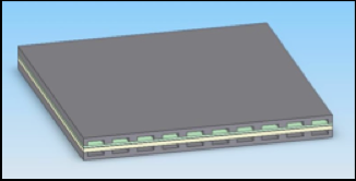
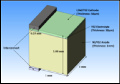
Fig. 19. (a) Planar SOFC architecture, and (b) unit cell used in the SOFC computational design.
Shown in figure 20 is the baseline unit cell, and unit cells of computationally optimized SOFCs with porous array microarchitectures in the anode, cathode, and cathode interconnect. The unit cell is 1mm x 1mm (l) x 1mm (w) x 1.06mm (h) with 1mm thick NiYSZ anode, 10µm thick YSZ electrolyte, and 50µm thick LSM cathode layers. The interconnects are 250µm wide, 1mm long and several mm thick. In these particular designs, the anode side has a vertical array of cylindrical pores terminating close to the anode-electrolyte interface, and the cathode side has a horizontal rectangular pore channel at the cathode-interconnect interface.
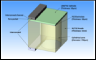
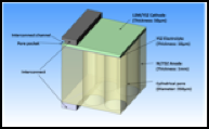
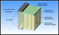
Fig. 20. Computationally designed unit cells with (a) single pore, (b) two by two pore array, and (c) three by three pore array in the anode layer, and a horizontal pore channel at the cathode/interconnect interface
Shown in Figure 21 is a SOFC button cell endowed with a porous micro architecture in the anode layer obtained through femtosecond laser ablation.
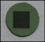
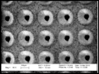
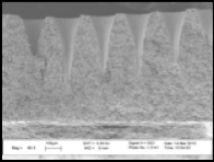
Fig. 21. (a) A 10mm SOFC button cell endowed with porous microarchitecture in the anode layer through hole drilling using femtosecond laser ablation. (b) A top-view SEM image of the hole drilled in the anode layer. (c) A SEM image of the fracture surface through the holes, showing the depth and profile of drilled holes.
3.2 Future Research: Direct Digital Manufacturing of Computationally Optimized SOFCs
Future research efforts will be directed towards prototyping and scale-up manufacturing to make commercial size SOFC plates with sizes on the order of 10cm x 10cm. Microarchitectured SOFC designs provide opportunities for further improvement through a hybrid approach involving incorporation of nanoparticles or thin films of catalysts inside our designed porous channels. Such an approach has the potential for simultaneously increasing reactant gas mass transport through the electrodes and overall surface area of catalyst thereby increasing the number of sites for electrochemical reaction, and the reaction rate.
4. NANOTECHNOLOGY
4.1 Large-Area Maskless Nanofabrication Through Laser Interference Patterning
Progress in nanotechnology requires versatile nanostructuring techniques capable of patterning diverse materials including those not traditionally allowed in cleanrooms. Large-area maskless nanofabrication techniques that achieve patterning through photochemical or photophysical means can dramatically reduce or even eliminate the high costs and long processing times associated with cleanroom technology. Such techniques can directly produce nanostructures on functional materials or can produce templates for subsequent synthesis or growth of nanostructured materials. My group has conducted research on one group of such techniques, known as laser interference patterning (LIP), which is an excellent technique for producing periodic micro- and nanostructures over large areas. A schematic of a LIP experimental setup is shown in Figure 22. As shown on the right of this figure, two-beam interference leads to periodic line-like intensity distribution while three-beam interference leads to an intensity distribution resembling periodic peaks and valleys.
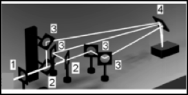
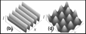
Fig. 22. Schematic setup for a three-beam laser interference system: nanosecond pulsed Nd:YAG laser with wavelengths of 1064nm, 532nm, 355nm, and 266nm (1) lens, (2) beam-splitters, (3) mirrors, (4) sample. The simulated intensity distributions of two-beam and three-beam interference are shown on the right.
When LIP is used for patterning photosensitive materials such as photoresists, it is known as laser interference lithography (LIL). When used for melting, it is termed laser interference melting (LIM), and when it used for ablation, it is known as laser interference ablation (LIA). My group has investigated all the above three modes of LIP to pattern photoresists, semiconductors, and metals to create diverse nanostructures. Some of the key examples are shown in figures 23-25 below.
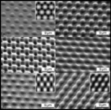
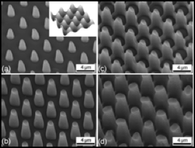
Fig. 23. (A) LIL of pentaerythritol triacrylate (PETIA) with three-beam interference. (B) LIL of polyethylene glycol diacrylate (PEGDA) hydrogel.
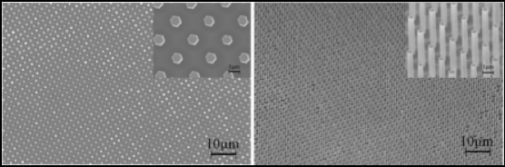
Fig. 24. Periodic ZnO nanowires grown through periodic holes produced in a photoresist through LIL.
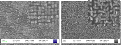
Fig. 25. Periodic bundles of carbon nanotubes grown on islands of iron catalyst patterned through LIA.
4.2 Future Research: Large Area Multiscale and Hierarchical Maskless Micro- and Nanomanufacturing
Future advances in nanotechnology will require the ability to pattern and process materials at the micro- and nanoscale over large areas rapidly, without masks in non-cleanroom type of setting. These advances will also require the capability of patterning hierarchical multiscale structures in diverse materials. This will require the design of sophisticated processes and material systems. In the future, I aim to investigate hybrid approaches that combine UV photopatterning, laser interference patterning, and block-copolymer lithography to create a unique methodology for generating hierarchical micro- and nanostructures with dual and triple length scale feature size and periodicity over very large areas, from wafer-scale up to areas approaching those for roll-to-roll processing.